Engineering the path from sensing to intelligent silicon
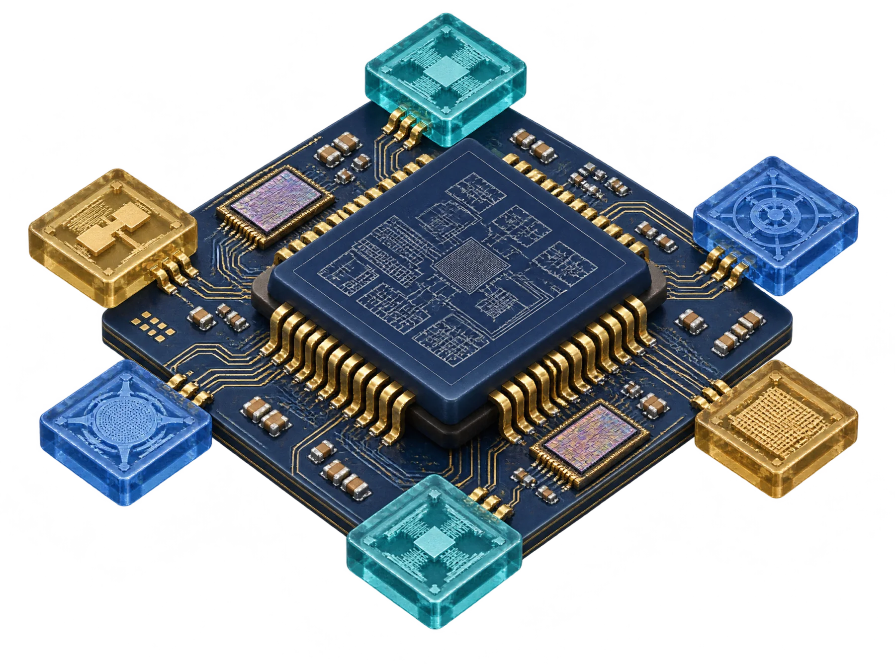
Santech develops MEMS sensing and mixed-signal semiconductor platforms, connecting U.S. research and architecture with engineering in India. Our JCB and Albert programs bring together sensing, signal processing and embedded intelligence for real-world applications.
 IIT Kharagpur
 TechUnited:NJ
 U.S.-India Business Council
 CMAI
Technology pathway
From product definition to tape-out and qualified silicon
Product definition
Translate the use case into sensor specifications, interfaces, PPA targets and reliability requirements.
MEMS + analog IP
Characterize the sensing element, low-noise AFE, ADC or frequency readout and calibration model.
SoC architecture
Partition reusable mixed-signal IP, embedded processing, security and system connectivity.
Verification + tape-out
Close simulation, functional verification, DFT, physical sign-off and MPW or tape-out readiness.
Package + qualification
Coordinate OSAT, bench characterization, reliability screening and customer qualification.
Core product programs
JCB and Albert: coordinated development programs
JCB (Jagdish Chandra Bose) is developing the sensing and instrumentation layer. Albert is defining a reusable mixed-signal architecture to connect those signals to applications.
Explore both programs
Our U.S.–India initiatives
Connecting research to a semiconductor ecosystem
From a proposed U.S. Centre of Excellence to phased campus initiatives in West Bengal, Santech's strategy brings together research, product development, talent and commercialization.
Explore the U.S.–India strategy
Applications for sensing and intelligent systems
JCB and Albert bring together sensing, mixed-signal electronics and embedded processing for applications across six industries.
 Healthcare & medical
 Industrial automation
 Environment & energy
 Automotive & mobility
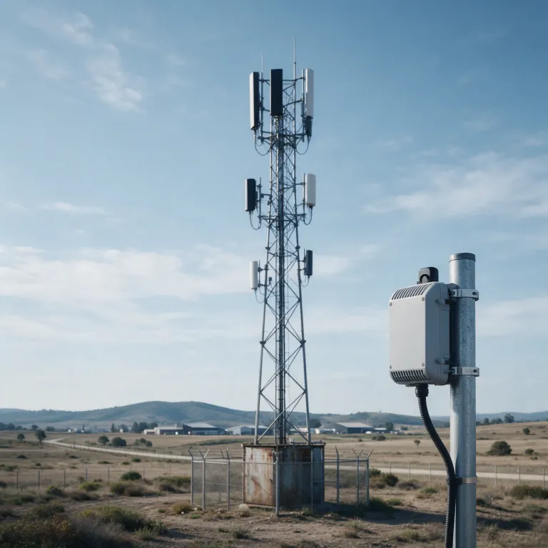 Telecom & connected IoT
 Aerospace & strategic systems

Santech - IIT KGP (Kharagpur) Research Center
MEMS research with IIT Kharagpur
Santech sponsors applied MEMS research at IIT Kharagpur, connecting sensing structures, prototype data and mixed-signal electronics with defined product programs.
Explore the research model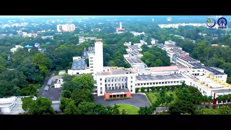
Engineering work
Engineering detail from Santech programs
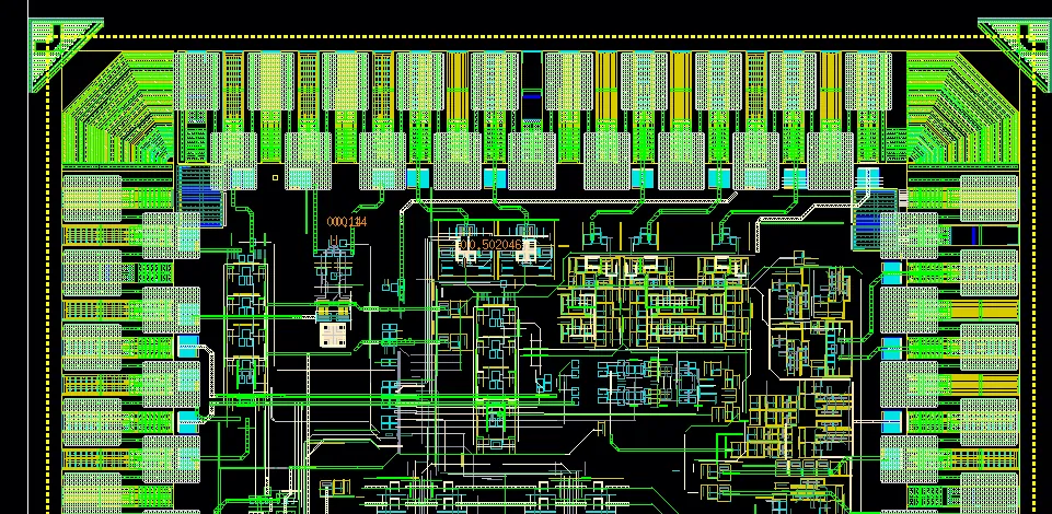
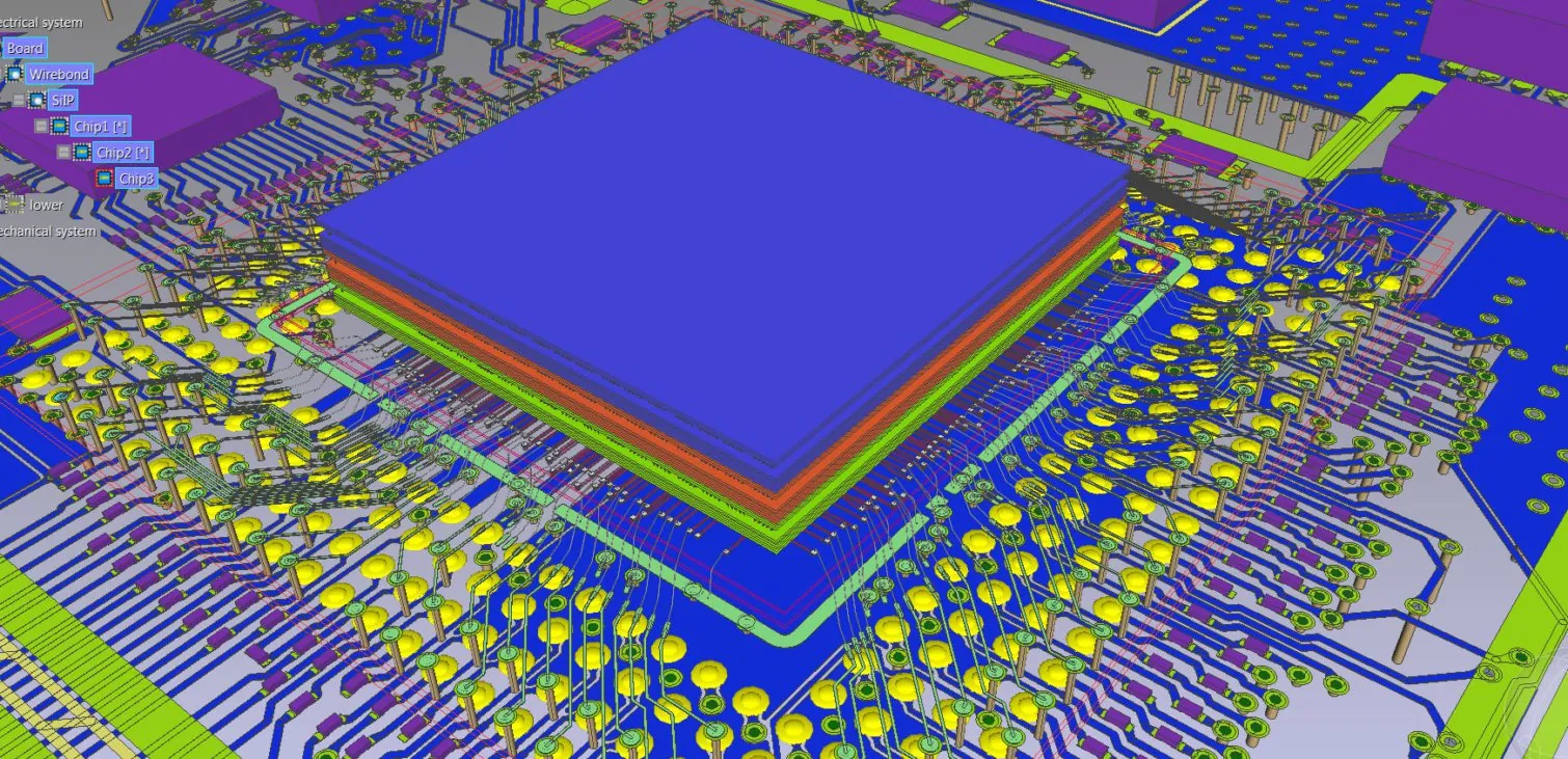
Explore the engineering behind integrated circuits, packages and board-level systems.